

Clear electronics/RF guides, videos & downloads by Ian Poole | Resource hub for engineers & hobbyists | Shop: https://nitter.cf/t.co/ClrsfjiAbA
South East, England
Joined November 2016
- Tweets28.5K
- Following269
- Followers17.5K
- Likes2.5K






4 Essential Things You Should Know About Zener Diodes
In this video, I cover 4 essential rules for designing reliable Zener circuits, including calculating the correct series current-limiting resistor and how to do this.
I also explain about maintaining sufficient current flowing through them and the reasons for this.
I also look at leaving safety margins for variable loads.
Plus, discover the physics behind the 5.1V to 5.5V temperature coefficient "sweet spot" and I explain why this occurs.
While Zener diodes aren’t always the most high performance voltage references, they are cheap, easily available and most of us have some available for quick circuits.
On top of this they are very easy to use!
Watch my video now to discover these essential secrets: youtu.be/4wWAkAWQTpM
#zener #zenerdiode #circuitdesign #HardwareDesign #HardwareEngineering #voltageregulator #voltagereference #electroniccomponents #electronicsnotes

Pen Multimeter Test: Is It Worth the Money?
My first look at the ANENG A3008 digital multimeter.
Boasting AC & DC voltage and resistance with auto-select, as well as capacitance, continuity, diode test, frequency, and even temperature - oh and I forgot the non-contact voltage measurement.
With 6000 count resolution and a reasonable accuracy on top of the 10Mohm impedance, this pen DMM is worth looking at.
Check my video: youtube.com/shorts/v9xtGZCnW…

Why are NPN transistors more widely used than PNP?
While both NPN and PNP bipolar junction transistors (BJTs) are essential tools for engineers, NPN versions are significantly more popular.
If you’ve spent any time looking at datasheets or schematics, you’ll notice they dominate the landscape.
Based on insights from Electronics Notes, here are the three primary reasons why NPN is the go-to choice:
1. Faster Performance (Carrier Mobility)
The biggest technical advantage comes down to physics. NPN transistors use electrons as their majority charge carriers, while PNP transistors rely on holes.
• Electrons move much more freely and quickly through the crystal lattice of the silicon than holes do.
• This higher "mobility" means NPN transistors can switch faster and provide better performance in high-frequency applications.
2. Standardized Negative Grounding
In the world of electronics—from automotive systems to consumer gadgets—negative grounding has become the universal standard.
• The polarity of NPN transistors is naturally compatible with negative ground configurations.
• This makes them easier to integrate into standard circuit designs without needing complex power supply arrangements.
3. Lower Production Costs
Manufacturing economics play a huge role. Most silicon-based components are most efficiently produced using large N-type silicon wafers.
• Interestingly, producing a PNP transistor with equivalent performance to an NPN often requires nearly three times more surface area on the wafer.
• Since wafer space is at a premium, this makes PNP transistors more expensive to manufacture, driving the industry toward the more cost-effective NPN alternative.
The Bottom Line:
While PNP transistors are still vital for specific tasks (like push-pull amplifiers or high-side switching), the NPN transistor's speed, compatibility, and cost-efficiency make it the undisputed heavyweight champion of the bipolar world.
For more information, check out the link to my website in the comments.
#Electronics #electroniccomponents #ElectricalEngineering #TechTips #Transistors #NPN #PNP #electronicsnotes

Check out the full breakdown of how these components work here: electronics-notes.com/articl…
This amazing digital multimeter comes in the shape factor of a pen. How useful!
The pen format for a DMM is particularly useful, because the measurement display is very close to the probe tip, so it is very much easier to probe and see the reading without taking your eyes away from the item under test and slipping with the probe..
With a 6000 count and the ability to measure AC & DC voltage, resistance, continuity, diode test, capacitance and more, this DMM is a must-have.
Also the meter is a very capable DMM with 6000 count resolution and great level of accuracy - quite sufficient for most electronics applications.
Check it out now!
Sponsored links:
Amazon. com: link.amazon/B0e9yVvQC
AliExpress: s.click.aliexpress.com/e/_c2…

Do You Know What a Transistor Current Mirror Circuit is & How It Works?
Transistor current mirror circuits are often used within integrated circuits as well as a number of other areas where they enable current to be balanced between two legs of a circuit.
Current mirror circuits generally consists two transistors, although other devices such as FETs can be used. Some current mirror circuits may use more than two transistors to enable the level of performance to be improved.
The current mirror circuit gains its name because it copies or mirrors the current flowing in one active device in another, keeping the output current constant regardless of loading.
The current being mirrored can be a constant current, or it can be a varying signal dependent upon the requirement and hence the circuit.
Conceptually, an ideal current mirror is simply an ideal inverting current amplifier that reverses the current direction as well or it is a current-controlled current source (CCCS). The current mirror is used to provide bias currents and active loads to circuits.
For more information check the link in the comments.
#transistor #circuitdesign #currentmirror #HardwareDesign

How to use a Spectrum Analyzer: the key elements.
Spectrum analyzers are probably the most important piece of test equipment for any RF testing, used in design, verification & validation, production test, maintenance and repair and many other RF associated investigations.
Spectrum analyzers can be daunting test instruments when they are first encountered, as their mode of operation may not be quite the ‘norm’ for many people.
But with a little understanding they give a whole new view on RF signals, and hence the RF circuits.
In this video, I detail what a spectrum analyzer is, what the controls are and how to use one.
Check out the video now: youtu.be/WnKK11UEvVE
#spectrumanalyzer #spectrumanalyser #RFtest #RFdesign #electronicsnotes #testmeasurement

Gallium Nitride GaN FETs Explained: do you really know what they are & how they work?
Gallium nitride is a semiconductor material that is being used increasingly to provide improved performance especially in high speed and RF FETs.
The very high electron mobility of gallium nitride, GaN enables the fabrication of semiconductor devices that have a low value of ON resistance combined with a very high switching frequency capability.
These benefits mean that GaN FETs are being used in many new electronic circuit designs for everything from power systems, for electric vehicles and renewable energy applications to RF power amplifiers, other RF design circuits and the like.
GaN FETs use the interface between two semiconductor materials to produce a very thin region known as the 2DEG to provide very high levels of electron mobility that result in GaN HEMTs or high electron mobility transistor being formed. GaN FETs are actually HEMTs although the HEMT term is rarely used.
Often GaN transistor technology is used to fabricate monolithic microwave ICs, MMICs which provide high levels of performance at microwave frequencies.
Check out the link in the comments for a fuller explanation.
#GaN #GaNFET #GanFETs #electroniccomponents

ANENG A3008 Pen Digital Multimeter Review - what is it like.
This DMM boasts a 6000 count solution and quite reasonable accuracy. It also has auto detect for AC and DC voltage and resistance .
It also measures capacitance, continuity (buzzer), temperature and non-contact voltage detection.
It’s basically a great little DmM for not a lot of money.
Watch my video now: youtube.com/shorts/v9xtGZCnW…

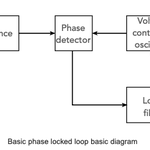
When designing Phase Locked Loops, the filter is probably the most key element in the circuit.
It defines elements like the loop stability, the bandwidth, capture rate, phase noise profile and much more.
Its design is a balance between all these parameters and it is one of the aspects that makes phase locked loop design so interesting.
Check out the full breakdown here: electronics-notes.com/articl…
#phaselockedloop #PLL #RFdesign

Zero-loss X-capacitor discharge technology just got an upgrade.
Reducing no-load standby power without adding design complexity is a constant challenge for power supply designers—especially when meeting strict standards like ErP Lot 6 or aiming for true ultralow standby consumption.
Power Integrations has introduced CAPZero™-4, the 4th generation of their pioneering X-capacitor discharge IC family!
By automatically disengaging the bleed resistors during normal operation and only connecting them when AC power is removed, CAPZero-4 consumes less than 1 mW (under 0.75 mW at 230 VAC). This frees up to 1000 mW of available standby power for the system load.
Key Highlights for Engineers:
🔹 Ultralow Consumption: Enables zero-watt no-load operation for AC-DC converters.
🔹 Drop-in Compatible: Pin-to-pin and package compatible with CAPZero-3 for effortless design migration.
🔹 Extended Thermal Range: Rated from -40 °C to 125 °C for demanding industrial and outdoor applications.
🔹 Global Safety Compliance: Certified to IEC 60335, EN/IEC 62368-1, UL 62368-1, and GB 4943.1.
🔹 Broad Application:Supports X-capacitance from 100 nF up to 6 µF across home appliances, displays, adapters, and industrial power supplies.
With over 1 billion CAPZero ICs shipped since 2010, this generation makes it even easier to meet stringent energy regulations while keeping BOM and layout changes to a minimum.
#PowerElectronics #HardwareDesign #PowerSupply #EnergyEfficiency #Semiconductors #Engineering #ACDC

Multilayer ceramic capacitors, MLCCs are one of the most widely used components these days.
Primarily in they are seen as surface mount components, but there are also leaded varieties.
Find out more in my video: tiktok.com/@electronicsnotes…
@ceramiccapacitors #capacitors #electronicsnotes

Is a Schottky diode the answer to your Power Efficiency & RF Sensitivity Circuit Problems?
A Schottky Diode can be the answer to high-speed switching and many other electronics circuit design performance issues. But it does have some issues.
If you’re designing a power supply or a high-frequency circuit, the "standard" diode might not always be your best option.
Selecting the right electronic component is key. Choosing between a PN Junction and a Schottky Diode can be the difference between it performing well, or not working as you want.
Here is the breakdown of the three "Big Dividers":
1. Forward Voltage (V_f)
* Standard PN: Typically drops about 0.7V. It’s the reliable workhorse, but that voltage drop turns into heat.
* Schottky: Uses a metal-semiconductor junction to achieve a much lower drop, usually 0.15V to 0.45V.
* The Result: Higher efficiency and less wasted power.
2. Switching Speed & Recovery
* Standard PN: These suffer from Reverse Recovery Time. When you switch them off, electrons have to "recombine," causing a brief lag.
* Schottky: They are majority carrier devices. There is virtually no stored charge to dissipate, meaning they switch almost instantaneously.
* The Result: Essential for high-speed switching and RF applications.
3. Reverse Leakage & Voltage
* Standard PN: High "blocking" capability (can handle 1000V+) and very low leakage current.
* Schottky: They are notoriously "leaky" at high temperatures and generally have lower breakdown voltages (usually capped around 100V or a little more for silicon Schottkys).
* The Result: If you need to block high voltage reliably, stick with Silicon or use silicon carbide Schottky diodes.
Where are they used?
* Standard PN Junction: general rectification, high voltage applications, general purpose circuits
Schottky Diode: power supplies, solar panel circuits, RF mixers, RF signal detectors, logic ICs
Pro Tip: Always check your thermal overhead. A Schottky’s low forward voltage is great, but if your environment is already hot, that increased reverse leakage can rocket upwards.
Where have you used either of these diodes?
#diodes #Semiconductors #PowerElectronics #electroniccomponents #TechTips #electronicsnotes

Check out my video explaining more: Schottky Diodes Unpacked: Low Voltage Drop, High Performance -
youtu.be/JBmSv2kitWM

Transistor Common Emitter Amplifier - the most versatile circuit?
The transistor common emitter circuit configuration is used for transistor circuit design. But how useful really is it?
In this video, I explain all about the common emitter amplifier: what it is, its advantages and see some circuit designs.
The transistor common emitter amplifier is probably the most widely used transistor configuration.
First of all, I explain what the Common Emitter Amplifier actually is: it's a circuit that uses a transistor, to amplify an input signal. The "common emitter" part refers to the fact that the emitter terminal is common to both the input and output circuits.
Next I look into how it works: when a small input signal is applied to the base of the transistor, it causes a much larger current to flow through the collector to the emitter. This results in a significant amplification of the input signal.
Here's a list of its chief characteristics:
a) It has a high voltage gain making it ideal for various applications.
b) It offers a moderate input impedance, allowing it to be driven by a variety of signal sources.
c) It has a medium output impedance and this makes it suitable for driving many loads.
Where is it used?
1) As general amplifiers for amplifying everything from audio signals, to almost anything.
2) In RF circuits for amplifying signals in communication systems in both transmitters and receivers
3) They can even be configured as oscillators by providing the right kind of feedback.
The common emitter amplifier is a versatile and fundamental circuit in electronics. Its ability to amplify signals effectively makes it an essential component in numerous electronic devices.
Check out my video now: youtu.be/A0sWlW1o0h0
#transistor #commonemitter #amplifier #circuitdesign #HardwareDesign #HardwareEngineering #electronicsnotes

Reed Relays are a Surprisingly Good Switching Solution.
Ever wonder how electronic circuits achieve fast, reliable, and isolated switching without the bulk of traditional electromechanical relays?
Meet the reed relay - a compact component that bridges the gap between traditional mechanical relays and solid-state alternatives.
What is a Reed Relay?
At its core, a reed relay consists of a reed switch - two overlapping nickel-iron blades hermetically sealed inside a glass envelope filled with inert gas (like nitrogen)—wrapped inside an electromagnetic actuating coil.
When current passes through the coil, it creates a magnetic field that magnetizes the blades. They attract each other, snap shut, and close the circuit. Remove the current, the field drops, and the spring-loaded contacts snap back apart.
Why Engineers Choose Reed Relays:
* Speed: Because the gap between contacts is tiny (0.05 to 1 mm), they boast incredibly fast switching speeds—often between 0.5 to a few milliseconds.
* Reliability & Longevity: Sealed inside glass, the contacts are entirely protected from moisture, oxidation, and contaminants.
* Complete Isolation: They offer absolute physical isolation between the control circuit (coil) and the switched circuit.
* Compact Size: They are small enough to fit into standard SIL or DIL integrated circuit packages, saving precious PCB real estate.
Design precautions:
While they are highly reliable, reed relays aren't always a "set-and-forget" component. When designing them into your circuits, remember:
1. Contact Bounce: The contacts collide with high energy, causing minor "bounces." If switching capacitive or inductive loads, this can cause arcing and reduce contact life.
2. Magnetic Interaction: Unscreened reed relays can experience magnetic coupling. If placed too close together on a PCB, their fields can oppose one another, requiring a higher coil voltage to close.
Pro tip: Always look for reed relays with built-in ferrous metal screens to optimize efficiency and enable tight stacking!
3. Current Constraints: They are typically built for low-to-medium signal switching, not heavy-duty power applications.
From test and measurement matrix switches to automated telecommunication exchanges, the reed relay remains an elegant, trusted solution for modern hardware engineering.
More information- check the link in the comment.
#ElectronicsEngineering #HardwareDesign #CircuitDesign #ElectronicComponents #ElectricalEngineering #electronicsnotes

And also check out my video:
Inside the Reed Switch: How a Tiny Magnet Changes Everything
youtu.be/uCYTTKwsM0g

👉 Want to dive deeper into the history, construction materials (like rhodium and ruthenium coatings), and circuit design considerations? Check out the full guide here: electronics-notes.com/articl…