Analog IC Designer | Structural Approach in the AI Wave | Semiconductors & Power & Optics | https://nitter.cf/t.co/wL7xmQ1wVu
Silicon Valley
Joined January 2015
- Tweets2.1K
- Following1.6K
- Followers22.2K
- Likes3.7K








Pinned Tweet
Nutty Atlas is where I keep my research on the AI build-out, from power and interconnects to packaging and memory.
You can browse by topic or company. If you’re curious about how the technology works and what it means for investors, have a look around.
atlas.nuttycld.workers.dev/?…

When AI stocks feel shaky, it’s worth asking: “So, are the data centers actually getting built?”
Supply across North America’s major markets keeps growing, and vacancy is just 1.4%. But signs of delays are showing up too.
Which companies will bear the cost of those delays? And what do they mean for the pace of the broader AI infrastructure buildout?
I dug into construction progress, actual operations, and how companies are funding the wait.



Nutty retweeted

The central theme is cost per good chip: the article connects ASML parts pricing, High-NA lithography, and advanced bonding through productivity, yield, and manufacturing economics.
Shorter HBM stacks do not necessarily mean less packaging investment: TrendForce reportedly sees some customers considering 8-high instead of 12-high, potentially increasing base-die and per-stack testing demand for a fixed DRAM supply.
Optical testing must distinguish product defects from measurement error: FormFactor’s alignment and calibration technologies address false failures, while volume production also requires sufficient test throughput.
Nutty’s Research connects ten equipment developments to the manufacturing problems they address. Its distinction between GF’s interposer manufacturing and Amkor’s assembly and testing helps clarify each company’s role.
The connection to optical testing is clear: stable measurements are necessary to understand yield and improve manufacturing. Production adoption, repeat orders, and shorter test times will show how that need translates into equipment business.

Had lunch with @damnang2 and @PhotonCap today!
Got to see Damnang sporting a new look with sideburns and a beard. 😂
Figured his profile pic needed an update, so I took care of it!

Nutty retweeted

An insightful article by Nutty on the semiconductor equipment value chain! I highly recommend giving it a read.
You don’t need to memorize every process and company in the value-chain map below to understand the semiconductor equipment industry.
This article provides just enough background to make sense of 10 major news stories and understand what they mean for the companies involved.
🤖 Made with AI

Great questions, @aryamman_bhatia .
1. It varies enormously depending on the process node and application. On a mature node, a relatively straightforward chip could reach mass production within a year. For high-end products at 2nm and below, I'd say 2–3 years is a reasonable ballpark, sometimes longer. Of course, it really depends on the complexity of the design.
2. The challenge is that silicon actually has to be fabricated. Unlike software, where more computing power can dramatically shorten iteration time, there's a physical limit to how fast you can make a chip. Both are equally important, though. If we could dramatically shorten that cycle, perhaps GPUs, CPUs, and memory could get updated every few weeks, just like iOS. Wouldn't that be something? :)
3. MPW is a bit of a different track. It's mainly about cost efficiency for prototyping rather than speed. Depending on the shuttle schedule, turnaround time can actually be longer than a dedicated run. The fastest way to get silicon? Burn money! 😂 A dedicated hot lot can buy you some priority in the fab and shave off some time. Of course, that still depends on the queue, and there's only so much you can accelerate.

I know… but it’s just too addictive 😱. Ever since I started using ChatGPT, I finally understand why kings kept flatterers around.

As an analog/mixed-signal IC designer, I’d be lying if I said I’d never dreamed of working at SpaceX or Tesla. But there are practical realities that I’m sure many engineers can relate to, so for now, I’m cheering from the sidelines.
Still, posts like this always make me feel that pull again.
P.S. The “1 chip in 2 years vs. 10 per year” comparison is a bit apples to oranges. The former refers to design-to-volume-production latency, while the latter is about experimental design throughput. I’m sure most people in the industry recognize the distinction. But even cutting the former by 30%, let alone 50%, would be an extraordinary achievement.

More dangerous than quoting someone without permission is selectively quoting them in a way that distorts the original author’s intent and context. 😡

I demand a public explanation from @TechPowerUp and the author of the article, AleksandarK.
A publication specializing in computer hardware has a responsibility to accurately convey both the fundamentals of the technology it covers and the context of the reporting it cites.
Yet this article quoted portions of my expert call report without my permission, omitted an important qualification explicitly stated in the original, and added market commentary without providing supporting evidence.
As a result, my interview has been presented in a way that makes it appear to substantiate a company’s technological failure and weakening market competitiveness.
Other websites have already cited the article and repeated the same narrative. As the author of the original report, I am setting the record straight.
First, Samsung’s shipment of HBM samples using hybrid bonding was already publicly disclosed.
During its earnings call on January 29, 2026, Samsung stated that it had delivered HBM4 samples using hybrid copper bonding to major customers in the fourth quarter of 2025 and had begun technical discussions with them. This was also covered by the press at the time. It was public information well before my interview.
Second, why did you omit the qualification explicitly stated in my report?
I do not understand why you exaggerated the wording in my article to portray SK hynix as being so far behind technologically. My original article explicitly states:
“This is a judgment about sample development progress. The discussion also included reservations about the performance of Samsung’s samples, so I would not extend that judgment directly to an advantage in production yield or customer qualification.”
Did you actually read my article properly before citing it? Or did you simply take a short snippet from Twitter and let your imagination run wild without bothering to investigate? Is this really what passes for professional reporting at a publication specializing in computer hardware?
Third, what evidence supports connecting a gap in hybrid bonding development to current HBM market share?
HBM products currently being mass produced and sold do not use hybrid bonding. What, then, does a gap in hybrid bonding technology have to do with current market share? Why introduce market share figures toward the end of the article in a way that misleadingly suggests these changes are occurring because of a gap in hybrid bonding technology?
Which customer has required hybrid bonding for which specific HBM product? Is there evidence that orders or supplier allocations changed because a supplier could not meet that requirement? If you are discussing a future risk, shouldn’t you first explain the relevant product generation, the timing of adoption, customer requirements, and the limitations of existing processes?
It is reasonable to discuss whether hybrid bonding could affect competitiveness over the long term. But that does not justify presenting current market share figures as if they were evidence supporting that outlook. I would like to know the intent behind publishing an article like this, using a sensational headline and plausible sounding language while framing the claims as things that “could happen.”
I put the following questions directly and firmly to the author and the editorial team.
How thoroughly did you review my original interview report and the information publicly disclosed before it? How did you distinguish between the interviewee’s statements, my interpretation, and your own speculation? What reporting did you actually conduct yourselves? Why did you connect information about a technology’s development status to current market conditions in this manner?
In my view, the way this article is constructed distorts the context of my reporting and risks misleading readers. Do not use my name to lend credibility to your questionable interpretations that lack adequate support.
I demand a clear response from the author and the editorial team explaining why my reporting was reframed in this way.

Vicor’s stock has had quite a run lately, and the company has made a clever move: customers can pay for patent rights to use competing modules, then get a royalty discount if they also buy Vicor’s products.
It earns licensing income while giving customers a reason to buy its hardware. I took a closer look at how much profit this could actually generate.
$VICR


Nutty retweeted

I’ve spent 20 years designing silicon chips. Now I’m building Silicon Atlas to help readers understand what new AI hardware changes, what the evidence supports, and what it could mean for the industry.
Paid subscriptions are now open.
Expect deep dives connecting chip architecture, system constraints, and industry economics, plus follow-up analysis as the evidence develops.
Everything I’ve published so far stays free, and I’ll continue sharing free essays and insights here. If my work has been useful to you, I’d appreciate your support.
$10/month or $100/year.
siliconatlas.substack.com/su…

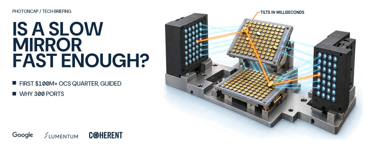
I happened to be working on an OCS article when @PhotonCap published this piece on the same topic.
It explains how skipping optical-to-electrical conversion can reduce costs and power consumption, and why slow-moving mirrors can still be fast enough for AI training. A useful look at both the technology and the economics behind Lumentum’s rapid OCS revenue growth.
My piece takes that discussion a little further, looking at how incumbents’ manufacturing experience stacks up against newcomers’ technologies. Coming soon.

I agree. The very term “goodput” implies delivering genuinely useful value, not just raw speed. Measuring it is far from simple, and inference companies will compete fiercely to prove it. With inference chips and racks only now reaching the market, we should soon see their real utility.

The competition in inference chips goes beyond speed. The system a customer chooses also determines which memory, networking components, and servers it buys.
In Part 2, I look at why customers might choose Cerebras or d-Matrix, how Jalapeño takes a different approach, and where companies like Broadcom and Celestica fit into these systems.