

All things 3D | Rendering | Simulation | Electronics | StartUp | CEO engineering services company - views are my own
Fürth, Deutschland
Joined October 2021
- Tweets1.6K
- Following267
- Followers25.9K
- Likes1K



Pinned Tweet
I am in the process of getting the production version of the open-source Raspberry Pi CM4 compatible module based on an iMX 8M plus up and running. If you are interested in this module, check out the Crowdsupply pre-launch page 😊


Snippet of the processing board hardware for the SDR dev kit. Boards are in production, complete units will be assembled in November 🙌


Based on the Framework SDR Module the TeraSDR dev kit will be available soon 🙌 Working on AoA, beamforming and beam nulling packages available with the system 👀


With the SiP now merged into the smartwatch mainboard design, I´m working on integrating the silicon-based power inductors into the new mainboard. These will be embedded inside the PCB. They are only ~200um thick so I´m running bow/twist simulation of the 0.5mm thick PCB to see if the internal stresses of the PCB could damage the inductors


Some more screenshots from letting Opus 5.5 route the smartwatch mainboard. I left out the GND layers as these are fully flooded plane layers. The component placement and fanout were pre-existin


Lukas Henkel retweeted

1/ I gave Opus 5.5 a single prompt to route a dense smartwatch PCB designed by @QVHenkel. Lukas graded the result a "4 out of 10". Here's how it went 🧵
I prototyped a black anodised case for the SmartWatch a while ago. Since I'm planning to integrate the BLE/WiFi antenna in form of a slot loop antenna into the frame, I ran some tests and for some reason the black anodised enclosure seems much more lossy than the one without any color in the oxide layer. I'm not sure yet what the reason is. It seems unlikely to me that a slightly conductive i.e. lossy (maybe carbon based ink?) would result in such an effect. I will investigate contact resistance first and remove the black anodisation from one of the prototypes around the area of the slot antenna with high field strength next. Potentially the batch with the black anodisation was also manufactured with a different aluminium alloy...


Added testpoints to the Smartwatch mainboard for the bring-up test jig. I'll have to prototype the pogo-pin setup next.


The smartwatch mainboard design is close to complete 🙌 I also tested a rendering AI rendering pipeline and it doesn´t look too bad in my opinion


Lukas Henkel retweeted

my dream of pcb renders in the style of Legend of Zelda Wind Walker is now complete.
altium cruncher "toon" is now available for kicking the tires. boards are rendered to svg for docs / cover art using a cell (cartoon) shading algorithm.
here is a demo w/ @QVHenkel 's open source PiMX8MP
dont let the 2d view fool you. this required a full 3d pipeline and some rather interesting algorithms to create.
the open source geometer library is doing the math with altium-monkey doing the file parsing.
github.com/wavenumber-eng/al…
I´ve looked at a few SMD power inductor geometries that are often used and not a single one needed a copper plane cutout underneath. Yes there are eddy current but they are very small. Also I´d rather have stray field contained this way
I have some older designs that I would approach differently nowadays. Wondering if there might still be use in publishing them even though they will be no longer manufactured/maintained


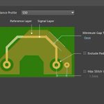
On many high-speed designs it is necessary to have a ground-plane void underneath large pads to minimize the local impedance dip.
I´ve used GPT-6 to create a script that reads the layerstack information through the Altium PCB API, isolate the target net- and pad class, creates an openEMS simulation, run the simulation to find the pad void size that does not create an impedance dip compared to the trace that is attached to the pad and ultimately apply the calculated GND void expansion value to all pads in a user-defined net class.
Currently all pads still receive the same expansion value. I will port the setup to use palace EM in order to automatically solve the expansion values for all different pad sizes/shapes in parallel which should be much faster than openEMS.
I´m not sure if this is a worrying trend with LLM generated designs. Due to the fact that the volume of open-source hardware designs is much smaller than say public code, it is much easier to inject false design philosophies into the training data of LLMs. This gets worsened by the fact that a large volume of open-source designs are from junior engineers and probably get weighed the same during training as a design e.g. from the open-compute project.
In this case it´s just an unnecessary high-frequency 100nF decoupling cap across a MicroSD card slot (not a knock against the designer) but the LLM probably took that from thousands of reference designs (in some cases probably even reference designs from chip vendors) and replicated it.
To be fair, many engineers would do the same just because it doesn´t matter (apart from cost and supply chain risk during an MLCC crisis like we had not long ago) but I would hope that an actual reasoning model at least in the future would be above that and judge by the physics and not take a volume of open-source design as the averaged standard. In the end everything we do in hardware is physics derived while all code frameworks at one point where thought into existence by humans and biased to some extent by the framework builders.
If this physics reasoning capability does not kick-in fast enough before more LLM generated designs flood the internet it might become problematic. It´s the classic dilemma that has been around since the fist LLMs of what happens if you train an LLM on LLM generated data but with e.g. code, images and videos the pool of input data is vastly bigger than open-source hardware designs so the impact will be noticeable much later. With hardware designs we might run into some actual effects of that problem much sooner.

