That's the power of Intel inside.
Joined October 2023
- Tweets2.3K
- Following250
- Followers2.2K
- Likes5.7K








The Inteller retweeted

What does it really take to make the world's most advanced chips?
Thousands of intricate manufacturing steps. Extraordinary engineering precision. And an industry working to meet growing global demand for computing.
Get an inside look at Intel's semiconductor innovation as Chris Auth, Pushkar Ranade, and other Intel experts join @dwarkeshpodcast to explore the science, technology, and manufacturing expertise behind advanced chips.
Watch the full conversation: ms.spr.ly/6014aaFMm
The Inteller retweeted

Foveros 2.5D enables high-density interconnects and heterogeneous chiplet integration, giving designers flexibility to combine different dies, process nodes, and IP in a single package.
Learn more: ms.spr.ly/6016aSNIQ
#IntelFoundry
The Inteller retweeted

Former Intel CEO Pat Gelsinger on getting hired at 18, designing Intel's chips while finishing his PhD, and arguing with his Stanford professors:
"I'm 16 years old. I accidentally win a scholarship. I go to tech school, skip my last year and a half of high school, and Intel comes recruiting when I'm 18 years old."
"The interviewer, he writes on his page, and I was number 12 that he interviewed that day... He says, 'Smart, aggressive, arrogant. He'll fit right in.'"
"I was engineer number four on the 386. Architect and design manager for the 486. All of that while doing my bachelor's, my master's and PhD work... Learning by day, and putting it to practice at night."
"One of the professors postulated a new carry lookahead adder design in one of my classes at Stanford. So I said, 'Well, I'm working on the 386 carry lookahead adder, so let me go try it.'"
"I come back two days later to the professor and I said, 'It doesn't work.' The next two class periods were just me and the professor arguing over why his design didn't work."
@PGelsinger @RaghuRaghuram @appenz

Former Intel CEO Pat Gelsinger with a16z's Raghu Raghuram and Guido Appenzeller on the next wave of semiconductor innovation and the physical constraints shaping the AI buildout:
Drawing on his experience designing Intel's 386 and 486 processors, Pat explains how AI could transform chip design, but also why faster design alone won't solve the industry's biggest problems.
They examine the bottlenecks in manufacturing, memory bandwidth, advanced packaging, and power, and why today's explosion of specialized AI chips may eventually consolidate around a smaller number of architectures.
They also discuss the potential for new memory technologies, the shift from copper to optical networking, and why energy capacity could become a major constraint on AI growth.
Finally, they revisit Pat's VMware years to ask what virtualization might look like when infrastructure is built for agents rather than humans.
YouTube: youtu.be/1Q_7yU7FZ1k
1:05 Hired by Intel at 18
3:50 Arguing with Stanford professors
7:25 Will AI design the next gen chips?
8:45 Designing faster than fabs can build
11:55 Why GPUs are stuck with bad memory
13:40 Why 100 AI chips will collapse to a few
19:15 Agents make new chips cheap to run
22:10 No new memory chip since the 90s
27:20 Why 16-layer chip stacks are a fantasy
32:15 The physics that keeps memory next to compute
34:55 "I declared the death of copper"
38:05 AI traffic breaks the internet's design
42:40 "Energy capacity equals economic capacity"
46:25 The 130-year-old power war AI reopened
48:50 VMware for agents
@PGelsinger @RaghuRaghuram @appenz
The Inteller retweeted

Not an expert but to the best of my understanding
One chart changed how I think about EUV.
I used to think EUV was only about making smaller chips.
But another benefit is simpler manufacturing.
Without EUV:
Print → Clean → Print → Clean → Print → Clean
With EUV:
Print → Clean
You still need cleaning, but far fewer times.
Less steps, less mistakes
3nm doesn't have 10× more mistakes.
It has roughly 10× more chances to make a mistake.
Think about it like this:
65nm: 100 cleaning steps
3nm: 1000 cleaning steps
If each step has a tiny chance of error, then doing 10x more steps creates many more chances for something to go wrong.
One mistake. Game over for the chip.
That's why advanced chip manufacturing is so hard.
Source: Nomura ANCHOR REPORT
China semiconductor equipment and materials

The Inteller retweeted

Intel presented some interesting details on #DiamondRapids at @hotchipsorg.
- Fabric Hub Tile: Intel 3
- Core Tile: Intel 18A-P
- Base Tile: Intel 3-T
For the package: Foveros 3D Direct and UCIe-S
hardwareluxx.de/index.php/ne…


The Inteller retweeted

Micron Technology's semiconductor buildout is taking shape on two fronts—and Boise is becoming a critical piece of the strategy.
➡️ Read more: brnw.ch/21x58fV
▪️Image: Micron Technology
#Semiconductors #AdvancedManufacturing
The Inteller retweeted

[Exclusive] SK hynix to Build Semiconductor Fab in Japan
SK hynix is moving forward with plans to invest tens of trillions of won to build a memory semiconductor fabrication plant (fab) in Miyagi Prefecture in northeastern Japan, according to sources familiar with the matter. If realized, it would mark the first large-scale investment by a South Korean semiconductor company to establish a local manufacturing base in Japan. However, as the Japan investment takes shape, U.S. pressure on Korean companies to expand memory production in the United States is also expected to intensify, further complicating their decisions over where to allocate future investment.
According to Hankyoreh’s reporting on the 20th, SK hynix is pursuing the construction of a memory semiconductor fab in Miyagi Prefecture, located in the Tohoku region of Honshu, Japan’s main island. A business community source said, “I understand that SK Group Chairman Chey Tae-won recently visited the area in person.” Miyagi is one of three regions, alongside Kyushu and Hokkaido, that the Japanese government is seeking to develop into major semiconductor industry hubs.
The investment is reportedly expected to amount to tens of trillions of won. Compared with the hundreds of trillions of won being invested in domestic semiconductor clusters in Yongin and the Honam region, the Japanese facility would represent a relatively smaller-scale production base. The Miyagi fab would be an additional overseas manufacturing site, while SK hynix proceeds with its planned domestic investments in the Yongin and Honam semiconductor clusters as originally intended. The move appears aimed at proactively expanding production capacity amid an ongoing global memory supply shortage.
If the plan materializes, SK hynix would become the third foreign semiconductor company, after U.S.-based Micron and Taiwan’s TSMC, to operate a semiconductor manufacturing facility in Japan. Samsung Electronics currently only operates an advanced semiconductor packaging research center in Yokohama.
However, the investment also carries risks. The United States has been pressuring the Korean government and Korean companies to invest in memory fabs on U.S. soil, and if SK hynix proceeds with its Japanese investment, Washington could intensify its demands for additional local production capacity in the United States. The company would also have to navigate domestic political uncertainty and public sensitivities in South Korea surrounding investment in Japan in a strategically important industry such as semiconductors.
The Inteller retweeted

Here’s an update on the @Tesla & @SpaceX joint Advanced Technology Chip Fab at Giga Texas (East Campus) … this is the R&D precursor to the huge TERAFAB ~ 100 miles (~ 165 Km) to the east.
This facility broke ground at Giga Texas in April 2026 & is meant for rapid vertical-integration prototyping of AI chips (Optimus, space compute & potential other future applications).
Foundation work continues to advance quickly, with GeoPiers, heavily reinforced footings, huge rebar cages, vertical structures & concrete pours underway, along with a strangely shaped large excavation.
This new facility is reported to cost ~ $3B & is both complementary & in addition to, the full-scale TERAFAB, located in Grimes County, TX , a roughly 100M+ sq ft, $16.8B just for Phase 1 (of eventually 10), aiming for 1TW+ annual compute.
This R&D pilot fab will develop the processes the TERAFAB will scale.


The Inteller retweeted
Terafab Construction Site & Land Plot Update:
The site is truly massive & only going to grow much larger as more land purchases are made. Right now, the total acreage owned is about 6,640 acres (2690 hectares) plus an additional 2,300 acres ( 930 hectares) that are in the final process of being recorded.
I estimate another 2,000 to 3,000 acres (800 to 1200 hectares) will need to be purchased for the final site.
On the east side of the Gibbons Creek Reservoir are the areas where land clearing is already underway.
Farther to the east along the spine of what will be Terafab, several other areas (shown in green) have been recently purchased, but the transactions have not yet been fully recorded. These newly acquired green areas mostly allow for the full length of the construction of Terafab, but not all of it.
There are many other land areas that will require purchasing as time goes on to be able to complete Terafab, likely including plots located between highway 30 & the construction site.
I think this will be a monumental construction effort & lengthy process until Terafab is fully completed.

The Inteller retweeted

More details on Nanya's EUV orders.
Nanya's board approved NT$346.6B (~$10.7B) for Fab 5A on August 5, its largest single project ever, with the first EUV-equipped wafer starts targeted for H2 2027.
The tell is in the guidance raise, the extra NT$17.7B added to 2026 capex is specifically for advance payments to secure ASML tool delivery slots, since EUV capacity is still supply-constrained.
Nanya will use use EUV on the 1–3 most pitch-constrained layers (active area/word line) on 1d/1e nodes while keeping DUV immersion multi-patterning everywhere else.
As a reminder, Nanya is 3-5 years behind , Samsung's been running EUV in DRAM since 2021, SK hynix just installed the first High-NA tool for DRAM in late 2025. This is Nanya usinh memory super cycle to buy its way back into the high end DRAM. Make the memory cycle longer and Nanya will have enough money to become a legit competitor to top four, able to capture more than it's current 1.6% share.
Last note but speculative: Nanya market cap is just $45B USD. If hyperscalars or larger non memory players have faith in elevated memory prices beyond 2030, someone should acquire Nanya.


The Inteller retweeted

$ASML EUV Units by Customer
"potential to raise 2028 0.33NA EUV capacity to 110 units (from 85 units in 2027). This is ahead of shipment consensus for 101 units."

The Inteller retweeted

Micron on Saturday broke ground on the expansion of its factory in western Japan, a ¥1.5 trillion ($9.3 billion) undertaking to produce advanced memory chips bloomberg.com/news/articles/…

The Inteller retweeted
Yesterday we celebrated the next chapter of Intel Mask Operations in Santa Clara.
Today, a closer look at why it matters: every advanced chip starts with a mask.
Learn how Intel Mask Operations helps turn chip designs into reality through industry-leading mask technology and manufacturing expertise.
#IntelFoundry


The Inteller retweeted

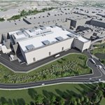
After a very long hiatus, @intel is once again expanding manufacturing operations in Santa Clara, right in the heart of Silicon Valley! Intel is committed to restoring American leadership in semiconductor manufacturing!