





Pinned Tweet
The new Q2 head: stereo cameras, stereo mics and speakers, and a frosted clear ring lit by 51 colour LEDs
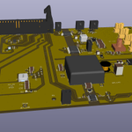
Q2 PCB refresh seems ready, and I was mostly the QA guy this time - opus was the one driving @kicad_pcb

Switched to grounded CAN shielding using @we_online WR-NPC2 thanks @Endreshazam


New face prototype for Q2. Boasting two @ArducamOfficial AR0234 global-shutter cameras (98° × 75° field of view) on a 54 mm stereo baseline. Each camera drops into a holder behind its lens and slides forward into a snug socket. The camera flexes run back along the neck to the adapter board, which sits on a removable hatch inside the neck, and a single ribbon goes on to the Jetson Orin. The head printed in PETG for a fit check, the final face panel will probably be CNC-machined in black POM-C.


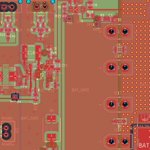
Agentic PCB tip #11: add a checker looking for dead-end fingers

I run ERC and DRC after every change, plus several additional checks:
1. Schematic parity (DRC with --schematic-parity)
2. Export the netlist and compare it against the baseline
3. Match each board pad’s net, pin name, and pin type to its schematic pin
4. Validate isolation domains: no inadvertent crossing
5. Validate that power-path widths were not narrowed inadvertently
6. Verify copper changes (diff tracks, vias, and zones)
7. Stale zone finder: refill the board and compare pours
8. Footprint geometry: verify position, shapes, and sizes
